
Date:
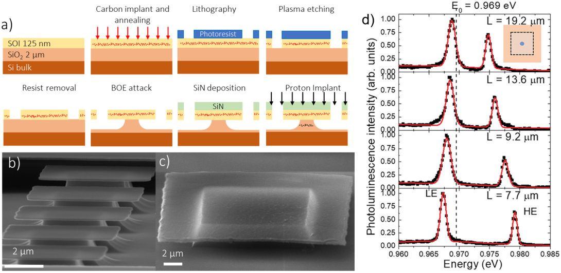
In a recent publication appeared on Advanced Optical Materials, scientists from an European collaboration led by prof. F. Biccari and prof. M. Abbarchi demonstrated a novel strain-based approach to tune the emission of silicon-based quantum emitters at telecom frequency. The work is the latest result of a collaboration between the Department of Physics and Astronomy of the University of Florence (NQSTI partner), the University of Aix Marseille, the National Institute of Photonics and Nanotechnologies of the National Research Council (NQSTI partner), and other European institutions. Light-emitting complex defects in silicon have been considered a potential platform for quantum technologies based on spin and photon degrees of freedom working at telecom wavelengths. Their integration in complex devices is still in its infancy and has been mostly focused on light extraction and guiding. In this publication the control of the electronic states of carbon-related impurities (G-centers) is addressed via strain engineering. Using thin silicon membranes embedding the emitters, and depositing a silicon nitride layer on top a tunable strain is applied. Symmetry breaking of the silicon crystal along [001] and [110] directions is demonstrated, resulting in a controlled splitting of the zero phonon line (ZPL), up to 18 meV. Some of the strained ZPLs are almost fully polarized, and their overall intensity is enhanced up to 7 times with respect to the flat areas outside the membranes. The merit of our approach is its simplicity, as it relies on conventional SiN deposition and lithography. It can be further engineered by changing patch geometry and orientation with respect to the crystallographic axes, SiN thickness and, most importantly, it can be easily extended to most common photonic devices. The full article by A. Ristori, M. Khoury, M. Salvalaglio, A. Filippatos, M. Amato, T. Herzig, J. Meijer, S. Pezzagna, D. Hannani, M. Bollani, C. Barri, C. M. Ruiz, N. Granchi, F. Intonti, M. Abbarchi, F. Biccari, "Strain Engineering of the Electronic States of Silicon-Based Quantum Emitters", is available here (https://doi.org/10.1002/adom.202301608 ).